
Unveiling the Hidden World of PCBs: Plated Through Holes, Blind Vias, and Buried Vias
Jul 28, 2023
Unveiling the Hidden World of PCBs: Plated Through Hole, Blind Via Hole, and Buried Via Hole
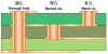
▍ Plated Through Hole (PTH):
A Plated Through Hole (PTH) is used to establish electrical connections between different conductive patterns in various layers of a printed circuit board (PCB). However, it cannot insert component leads or other reinforcing materials. A PCB is composed of multiple layers of copper foils stacked together. These copper layers are isolated from each other by insulating layers, necessitating signal links through via holes for connectivity. Hence, they are referred to as Plated Through Holes.
PTH is the simplest type of hole, as it involves drilling or laser-drilling the PCB to create through-holes directly. This method is relatively cost-effective. However, in some circuit layers, not all through-holes are required for connections, resulting in wastage. This is especially true for high-density interconnect (HDI) boards, where space is at a premium. Thus, while PTH is inexpensive, it may sometimes consume additional PCB space.
▍ Blind Via Hole (BVH):
Blind vias (BVH) connect the outermost layer of the PCB to the adjacent inner layer through plated holes. Since the other side is not visible, it is called a "blind" via. The emergence of the "blind hole" process is to improve the utilization of space in the PCB circuit layer.
Blind vias are located on the top and bottom surfaces of the PCB and have a specific depth, used for connecting surface traces with traces on inner layers. The depth of the holes typically follows a predefined ratio (aspect ratio). This manufacturing method requires careful attention to drilling depth to avoid difficulties in electroplating inside the holes. Consequently, it is not commonly used in manufacturing. Alternatively, it is possible to pre-drill the vias in individual circuit layers that need to be interconnected and then laminate them together. However, this approach demands precise alignment and positioning equipment.
▍ Buried Via Hole (BVH):
A Buried Via Hole (BVH) refers to connections between any internal circuit layers within a printed circuit board (PCB) without extending to the board's surface.
This fabrication process cannot be achieved by drilling after PCB lamination. Instead, the drilling operation must be performed in specific circuit layers first, followed by partial lamination, electroplating, and finally complete lamination. Due to the more intricate process compared to through-holes and blind vias, this method is the most expensive. It is typically reserved for high-density circuit boards to maximize space utilization in other circuit layers.

.png?x-oss-process=image/resize,w_100/quality,q_100)
Recent Posts

October 26, 2016
The Most Successful Engineering Contractor


May 12, 2025
China PCB Drilling Routing machine Development
May 06, 2025
PCB Design Process and Key PointsCONTACT US
Contact US
Product Information
Quantity
Unit
Piece
Support order samples, customization, wholesale direct, and complete payment. If the product you look for does not have corresponding customized content, pls fill out the form below to contact us, and we will reply ASAP.