
PCB Design Process and Key Points
May 06, 2025
When receiving printed boards from the manufacturer, all boards should be inspected, including mass-produced PCBs. Samples or first batches of printed boards should be fully inspected, and mass-produced PCBs should also be subject to at least one inspection.
In addition to inspecting the printed boards after each production process, the manufacturer should have a quality inspection process for the completed printed boards immediately to verify the quality of the printed boards, but whether the printed boards meet the specifications should be verified by the purchaser. Although many aspects cannot be verified, such as the materials and internal characteristics of the printed boards. However, many other aspects can and should be verified.
This article is brief, but it should be noted because of its importance. The information provided by the PCB board should be used on each printed board. Additional tests should be performed based on the application, complexity and requirements.
1. Why to inspect
Not all specifications require inspection, but history has shown that a few minutes of inspection can avoid hours of troubleshooting and repair, save hours of conversations with the manufacturer, and recovery costs and assembly costs.
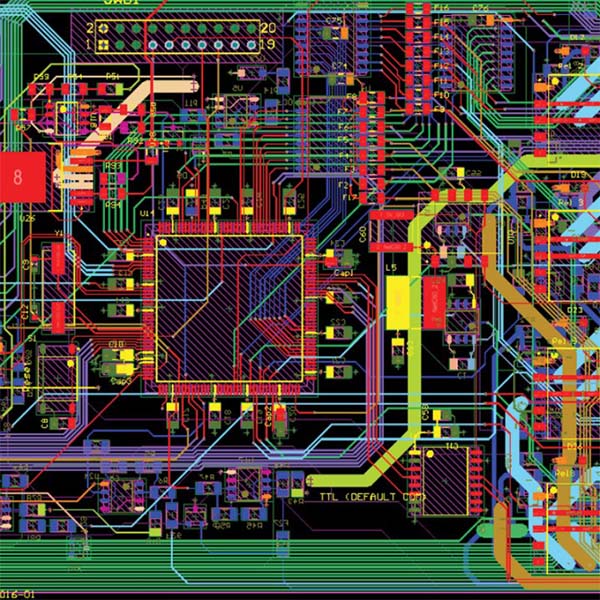
Next, enter the printed board inspection:
1. Visually inspect the printed board, paying attention to cleanliness and appearance. Check the solder mask,
Include: specified color, specified thickness, quality, stains, pitting, is the plating sufficient.
Plating
Whether the plating is sufficient is difficult to measure. The current requirement is based on the thickness of the plating. If the requirements are strict, the plating may become the key. The simplest method is to cover the area near the edge of the printed board in front of or beside a pad. The unmasked area will be used as a control point, so when the pad height/thickness is measured, this value can be subtracted from the thickness of the printed board and multiplied.
2. The above provides a method to measure the thickness of the copper/plating flow solder combination. Regardless of the plating thickness, the flow solder should be consistent.
The completed hole ring can be checked by rough observation, or with an eye ring, or a magnifying glass with an embedded size and sample diameter can be used to check. The completed hole ring should not be less than the specified hole ring, or the completed hole ring minus the manufacturer's 2A hole ring has enough clearance.
Hole wall drilling quality is important, but it is difficult to detect and verify. On all multilayer printed boards, manufacturers should implement cross-sectional testing. Upon request, the manufacturer should provide a certificate or copy of the inspection that has been done. A rough test can be used to check continuity. A multimeter should be used to measure the resistance of the electrical connection from the PLTH on one board to the PLTH on another board. The resistance should be less than 1Ω+1Ω/inch. A plane-to-plane test should be performed to verify that there are no shorts or internal contaminants. This value should be greater than 100MΩ when no components are assembled.
1. Are the layers aligned?
The obvious in-board reference points on each layer can be used to verify whether the layers are aligned, including the solder mask layer and the screen printing layer. The manufacturer of the PCB board can use these reference points during the alignment process.
2. Perform adhesion inspection.
Place a piece of tape on the plating/gold and remove it. If the plating layer or gold is carried away by the tape, the plating is not enough.
3. Does the appearance meet the production baseboard requirements?
Verify that the text and line positions are correct and that all holes are in the correct position (visual inspection). Make sure that all text thickness and line width are correct and that all additional annotations are correct. The actual result may not be the same as what is shown on paper, so this simple check can ensure that the result is as expected. In mass production, simple manufacturing errors (such as missing a mounting hole) may not be discovered until the printed board is assembled. A simple way to check for correctness is to superimpose a 1:1 drawing on the printed board. Using a film in the clearest format can also verify that the dimensions are correct.

Recent Posts

October 26, 2016
The Most Successful Engineering Contractor


May 12, 2025
China PCB Drilling Routing machine DevelopmentCONTACT US
Contact US
Product Information
Quantity
Unit
Piece
Support order samples, customization, wholesale direct, and complete payment. If the product you look for does not have corresponding customized content, pls fill out the form below to contact us, and we will reply ASAP.