
Technological Innovation and Intelligent in PCB Manufacturing
Apr 14, 2025
Technological innovation and intelligent manufacturing
High-end HDI board research and development: As chip manufacturing processes enter the 5nm or even 3nm era, traditional 5-level and 6-level HDI boards can no longer meet the needs of high-speed data processing. The industry is accelerating the development of higher-level HDI boards to improve the performance and signal integrity of PCBs.
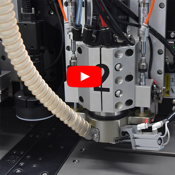
A high-performance PCB drilling machine with a CCD camera designed by CHIKIN.
|
Chikin Drilling and Routing Machine Special Features
|
|
|
Clamping heel of the treatment area
|
availability
|
|
The ability to adjust the cutting height
|
availability
|
|
Automatic tool change
|
availability
|
|
Automatic tool measuring system
|
availability
|
|
Automatic tool breakage control system
|
availability
|
|
Information about the tool's resource
|
availability
|
|
Pneumatic clamping of workpieces in the cutting area
|
availability
|
|
Graphical control of the tool store
|
availability
|
|
Editing inactive programs during processing
|
availability
|
|
The ability to store programs on a hard disk
|
availability
|
|
Fault messages
|
availability
|
|
CCD camera CCD
|
availability |
AI-driven defect detection: Researchers proposed a GAN-enhanced YOLOv11 model for detecting PCB surface defects such as missing holes, mouse bites, and open circuits. This method enhances the model's ability to identify complex and rare defects by generating synthetic defect images, and improves the accuracy and robustness of detection.
Global supply chain and market dynamics
Industry transfer to low-tariff areas: The Sino-US tariff deadlock has prompted the PCB industry chain to accelerate its transfer to low-tariff regions such as Southeast Asia. For example, Apple's PCB supplier Meiko plans to invest $350 million to build a factory in Vietnam to avoid the cost pressure brought by high tariffs.
Enterprise restructuring and integration: Aims to integrate resources and enhance competitiveness.
Sustainable development and environmentally friendly materials
Research and development of recyclable PCB materials: Researchers have developed recyclable PCB materials based on transesterified vitrimer. This material not only has the electrical and mechanical properties of traditional PCBs, but can also be non-destructively recycled through the swelling method, achieving a polymer recovery rate of up to 98% and a fiber recovery rate of 100%, significantly reducing the impact of electronic waste on the environment.


Recent Posts

October 26, 2016
The Most Successful Engineering Contractor


May 12, 2025
China PCB Drilling Routing machine Development
May 06, 2025
PCB Design Process and Key PointsCONTACT US
Contact US
Product Information
Quantity
Unit
Piece
Support order samples, customization, wholesale direct, and complete payment. If the product you look for does not have corresponding customized content, pls fill out the form below to contact us, and we will reply ASAP.