
Introduction to Equipment in PCB Production Lines
Mar 27, 2025
Introduction to Equipment in PCB Production Lines
Printed Circuit Boards (PCBs) are at the heart of virtually all electronic devices. From smartphones and computers to household appliances and medical devices, PCBs are essential components for creating functional and reliable electronics. A PCB production line involves several critical processes, from the design and fabrication to the testing and assembly of these boards.
This article aims to introduce the various types of equipment used in PCB production lines, outlining their purpose and importance in ensuring the quality and efficiency of the manufacturing process.
1. PCB Design Software and Equipment
Before the physical production of a PCB can begin, the design of the board must be completed. This process typically starts with the creation of a schematic diagram, followed by the PCB layout design. Various software tools are used in this phase to define the components' placement, the routing of electrical traces, and other critical parameters.
Key Equipment:
-
CAD Software: Tools such as Altium Designer, Eagle, and KiCad are used to design the PCB. These software platforms allow engineers to create detailed schematics, simulate electrical properties, and generate the files needed for manufacturing.
-
CAM Systems: Computer-Aided Manufacturing (CAM) software is used to convert PCB designs into machine-readable formats (Gerber files). These files guide the automated equipment on how to fabricate the PCB.
2. PCB Lamination Equipment
Lamination is a crucial step in PCB production, where the different layers of the PCB are bonded together. This process requires precise control of heat and pressure to ensure proper adhesion without damaging the underlying materials.
Key Equipment:
-
Lamination Press: This machine applies pressure and heat to laminate the copper-clad boards with the resin layers. The lamination press ensures that the layers are bonded securely without any air gaps or delaminations.
-
Autoclave: In some cases, autoclaves are used for lamination, especially when high-density PCBs or multi-layer boards are involved. The autoclave ensures a controlled environment for the lamination process, preventing defects and ensuring uniform bonding.
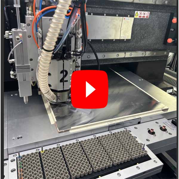
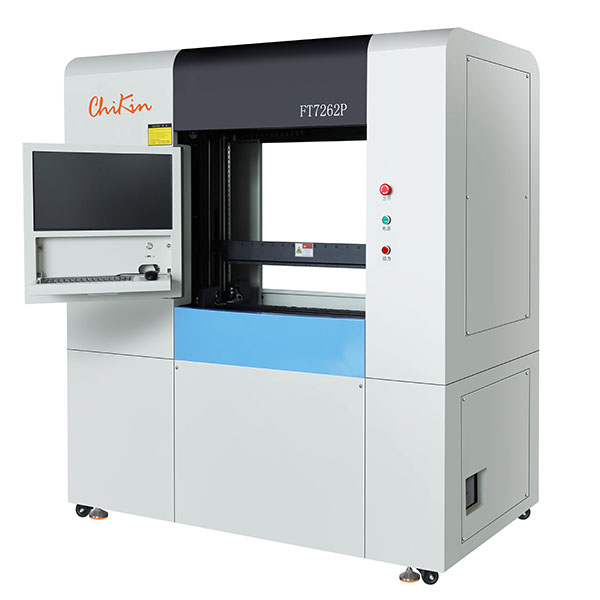
3. Drilling and Routing Equipment
Drilling is essential to create the vias and holes in a PCB for component mounting and electrical connections. The precision of this step is critical, as it directly impacts the functionality of the PCB.
Key Equipment:
-
Drilling Machine: These machines use high-speed rotating drills to create holes in the PCB. CNC (Computer Numerical Control) drilling machines are commonly used for precise and automated drilling of various hole sizes.
-
Laser Drilling Machine: In cases where microvias or finer holes are required, laser drilling machines can be used. They offer higher precision and can drill smaller holes than traditional mechanical drills.
-
Routing Machine: After drilling, a routing machine is often used to cut the PCB into its final shape. Routing also allows the creation of more complex shapes and contours, which is essential for customizing the design.
4. Copper Etching Equipment
Copper etching is a process used to remove unwanted copper from the surface of the PCB to create the required electrical traces. This process involves the use of a chemical solution that dissolves the excess copper, leaving only the designed traces behind.
Key Equipment:
-
Etching Machine: The etching process is typically carried out in a specialized etching machine that uses a mixture of chemicals, such as ferric chloride, to remove the unwanted copper. The PCB is passed through a series of tanks, each containing a specific solution.
-
Spray Etching System: This system uses a spray of etching solution to target specific areas of the PCB. It is often used for high-precision etching and is ideal for fine-pitch circuits.
5. Solder Mask and Silkscreen Printing Equipment
After the copper traces are etched, the PCB needs to be coated with a solder mask. The solder mask protects the PCB's copper traces from oxidation and prevents short circuits during soldering. Additionally, a silkscreen layer is printed on the board to mark component locations and other important information.
Key Equipment:
-
Solder Mask Coating Machine: This machine applies a thin layer of solder mask to the PCB. The solder mask is then cured under UV light to harden it.
-
Silkscreen Printer: A silkscreen printer is used to print text and symbols onto the PCB. This is often done using inkjet or screen printing techniques to ensure legibility and durability.
-
6. PCB Inspection and Testing Equipment
Once the PCB has gone through the initial manufacturing steps, it must be thoroughly inspected to ensure that it meets all design specifications and quality standards. Inspection and testing equipment are critical for identifying defects such as missing or misaligned components, incorrect solder joints, and electrical shorts.
Key Equipment:
-
Automated Optical Inspection (AOI): AOI machines use high-resolution cameras to inspect the surface of the PCB for defects in the copper traces, solder mask, and components. These machines can detect issues like missing components, improper component orientation, or soldering defects.
-
X-ray Inspection System: For multi-layer PCBs, X-ray inspection is essential for detecting internal defects such as voids in solder joints or problems with vias. X-ray machines provide a non-destructive way to inspect the inner layers of the PCB.
-
Electrical Testing (In-Circuit Testing and Functional Testing): These tests check the electrical functionality of the PCB. In-circuit testers (ICT) verify that each component is correctly placed and functioning. Functional testing ensures that the complete circuit behaves as expected under operational conditions.
7. Reflow Soldering Equipment
Reflow soldering is a key process in PCB assembly where solder paste is melted to create solid electrical connections between the PCB and its components. The process involves heating the PCB in a controlled manner to ensure the soldering process is precise and uniform.
Key Equipment:
-
Reflow Oven: This machine is used to heat the PCB to the required temperature for soldering. The PCB passes through a series of temperature zones in the oven, allowing the solder paste to melt and form strong, reliable solder joints.
-
Solder Paste Printer: Before reflow soldering, solder paste is applied to the PCB using a solder paste printer. The paste is applied precisely to the pads where the components will be placed.
8. Wave Soldering Equipment
For PCBs that contain through-hole components, wave soldering is often used to attach the components to the board. This process involves passing the PCB over a wave of molten solder, which forms connections with the through-hole leads.
Key Equipment:
-
Wave Soldering Machine: The wave soldering machine contains a molten solder bath, and the PCB is passed over the wave of solder to create the necessary connections. The wave soldering process is typically used for large batches of PCBs with through-hole components.
9. Assembly Equipment
Once the PCB is fabricated and soldered, the final step is the assembly of components. This process involves placing components like resistors, capacitors, and integrated circuits (ICs) onto the PCB.
Key Equipment:
-
Pick-and-Place Machine: This automated machine picks components from a tray or reel and places them onto the PCB. The pick-and-place machine is highly accurate and can handle components of various sizes and shapes.
-
Surface-Mount Technology (SMT) Line: SMT equipment is used for assembling surface-mount components. The SMT line includes several machines, such as solder paste printers, pick-and-place machines, and reflow ovens, to assemble the board efficiently.
-
Through-Hole Insertion Machine: For through-hole components, this machine inserts the leads into the PCB holes before soldering them into place.
10. Final Testing and Packaging Equipment
Once the PCB is fully assembled, it undergoes a final round of testing to ensure it meets all operational and quality standards. After testing, the PCB is packaged for shipment.
Key Equipment:
-
Functional Testing Equipment: This equipment tests the functionality of the fully assembled PCB, ensuring that all components work as expected.
-
Automated Packaging Line: The final PCB products are automatically packaged for delivery, with the packaging process involving labeling, vacuum sealing, and boxing for safe transportation.
The PCB production process is complex, involving multiple stages that require specialized equipment to ensure high-quality results. From the design phase to the final testing and packaging, each piece of equipment plays a critical role in ensuring the PCB is manufactured to meet the exact specifications of the design. As technology continues to advance, the PCB manufacturing process will evolve, with even more sophisticated equipment becoming available to handle increasingly complex and precise designs.
Understanding the different types of equipment involved in PCB production helps to highlight the level of expertise and precision needed to create reliable electronic products. Whether for consumer electronics, automotive, or medical devices, high-quality PCBs are essential for ensuring that modern electronics function as intended.

Recent Posts

October 26, 2016
The Most Successful Engineering Contractor


May 12, 2025
China PCB Drilling Routing machine Development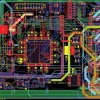
May 06, 2025
PCB Design Process and Key PointsCONTACT US
Contact US
Product Information
Quantity
Unit
Piece
Support order samples, customization, wholesale direct, and complete payment. If the product you look for does not have corresponding customized content, pls fill out the form below to contact us, and we will reply ASAP.