
Name Explanation of various PCB boards
Dec 06, 2022
Name Explanation of various PCB boards
In PCB field, there are a various kind of PCB boards, do you know what are they? Today, let’s have a look.
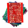
![]() PCB: Printed Circuit Board (PCB) refers to a printed board that forms point-to-point connections and printed components on a general-purpose substrate according to a predetermined design,its main functions are: 1) Provide mechanical support for various components in the circuit; 2) Make various electronic components form the electrical connection of the predetermined circuit, and play the role of relay transmission; 3) Mark the installed components with marking symbols, which is convenient for insertion, inspection and debugging.
PCB: Printed Circuit Board (PCB) refers to a printed board that forms point-to-point connections and printed components on a general-purpose substrate according to a predetermined design,its main functions are: 1) Provide mechanical support for various components in the circuit; 2) Make various electronic components form the electrical connection of the predetermined circuit, and play the role of relay transmission; 3) Mark the installed components with marking symbols, which is convenient for insertion, inspection and debugging.
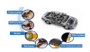
![]() Copper Clad Laminate (CCL for short): it is the core material for making printed circuit boards, and it is responsible for the three functions of conductive, insulating and supporting printed circuit boards. The quality of CCL determines the performance, quality, processability in manufacturing, manufacturing level, manufacturing cost and long-term reliability of printed circuit boards.
Copper Clad Laminate (CCL for short): it is the core material for making printed circuit boards, and it is responsible for the three functions of conductive, insulating and supporting printed circuit boards. The quality of CCL determines the performance, quality, processability in manufacturing, manufacturing level, manufacturing cost and long-term reliability of printed circuit boards.
![]() FR-4: flame retardant epoxy resin glass fiber cloth base copper clad laminate.
FR-4: flame retardant epoxy resin glass fiber cloth base copper clad laminate.
![]() HDI: The abbreviation of "High Density Interconnect", a high-density printed circuit board technology using thin lines, tiny holes, and thin dielectric layers.
HDI: The abbreviation of "High Density Interconnect", a high-density printed circuit board technology using thin lines, tiny holes, and thin dielectric layers.
![]() Rigid board: A printed circuit board made of a rigid base material that is not easy to bend and has a certain degree of toughness.
Rigid board: A printed circuit board made of a rigid base material that is not easy to bend and has a certain degree of toughness.
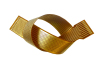
![]() Flexible board (FPC): also known as flexible board, is a printed circuit board made of flexible insulating substrates such as polyimide or polyester film. The flexible board can be bent, wound and folded, and can be arranged according to the requirements of the space layout, and move and expand in three-dimensional space, so as to achieve the integration of component assembly and wire connection.
Flexible board (FPC): also known as flexible board, is a printed circuit board made of flexible insulating substrates such as polyimide or polyester film. The flexible board can be bent, wound and folded, and can be arranged according to the requirements of the space layout, and move and expand in three-dimensional space, so as to achieve the integration of component assembly and wire connection.
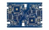
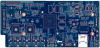
![]() Multi-layer board: multi-layer board is a printed circuit board with four or more layers. The multi-layer single-sided or double-sided boards are hot-pressed together, and through secondary drilling and hole metallization, formed between different layers. Conductive pathways.
Multi-layer board: multi-layer board is a printed circuit board with four or more layers. The multi-layer single-sided or double-sided boards are hot-pressed together, and through secondary drilling and hole metallization, formed between different layers. Conductive pathways.
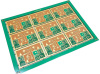
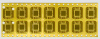
![]() IC Package Substrate: the package substrate is the key carrier of the packaging and testing link of the integrated circuit industry chain. It can achieve multi-pin, reduce the area of packaged products, improve electrical performance, and achieve high density.
IC Package Substrate: the package substrate is the key carrier of the packaging and testing link of the integrated circuit industry chain. It can achieve multi-pin, reduce the area of packaged products, improve electrical performance, and achieve high density.
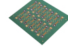
![]() SLP (substrate-like PCB): It is the main force of the next generation PCB board. Compared with the HDI board, it can be more detailed, and can shorten the line width/space from HDI's 40/50 microns to 20/35 microns. From the perspective of manufacturing process, SLP is closer to the IC substrate used for semiconductor packaging, but it has not yet reached the specifications of the IC substrate. However, its purpose is still to carry various active and passive components, so it still belongs to the category of PCB, and the number of electronic components in the same area can reach twice that of HDI.
SLP (substrate-like PCB): It is the main force of the next generation PCB board. Compared with the HDI board, it can be more detailed, and can shorten the line width/space from HDI's 40/50 microns to 20/35 microns. From the perspective of manufacturing process, SLP is closer to the IC substrate used for semiconductor packaging, but it has not yet reached the specifications of the IC substrate. However, its purpose is still to carry various active and passive components, so it still belongs to the category of PCB, and the number of electronic components in the same area can reach twice that of HDI.

Recent Posts

October 26, 2016
The Most Successful Engineering Contractor


May 12, 2025
China PCB Drilling Routing machine Development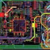
May 06, 2025
PCB Design Process and Key PointsCONTACT US
Contact US
Product Information
Quantity
Unit
Piece
Support order samples, customization, wholesale direct, and complete payment. If the product you look for does not have corresponding customized content, pls fill out the form below to contact us, and we will reply ASAP.