
HDI Technology and PCB Miniaturization: Key Drivers of Innovation in Modern Electronics
Oct 24, 2024
HDI Technology and PCB Miniaturization: Key Drivers of Innovation in Modern Electronics
8
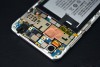
In today’s rapidly advancing technological landscape, printed circuit boards (PCBs) are a critical foundation for modern electronics, serving as the "nervous system" that enables devices to operate efficiently and reliably. As industries such as consumer electronics, telecommunications, and healthcare push the boundaries of innovation, the demand for smaller, more powerful, and more efficient electronic devices has never been higher. This need has led to significant advancements in PCB miniaturization and High-Density Interconnect (HDI) technology, which are becoming key enablers for next-generation products.
In this article, we will explore the factors driving PCB miniaturization, the role of HDI technology in meeting these demands, the manufacturing challenges, and its implications across different industries.
8
1. The Driving Forces Behind PCB Miniaturization
a. Consumer Electronics and Portable Devices
The consumer electronics industry is perhaps the most visible driver of PCB miniaturization. With the rise of smartphones, wearable devices, and IoT (Internet of Things) gadgets, consumers are expecting devices to become not only more powerful but also smaller and more portable. As devices shrink in size, the components inside them must follow suit. This demand is pushing PCB manufacturers to create smaller and denser circuit boards that can fit into increasingly compact product designs without compromising functionality.
For example, modern smartphones have evolved to pack advanced features such as multiple cameras, high-speed processors, and large battery capacities, all within slim and lightweight casings. Miniaturized PCBs with HDI technology make it possible to integrate these components efficiently, allowing for the compactness and complexity that consumers now take for granted.
8
b. Automotive and Aerospace Applications
The automotive industry is undergoing a transformation with the introduction of electric vehicles (EVs) and autonomous driving technologies. These systems require high-performance, reliable, and compact PCBs to control and manage a wide array of electronic functions, from in-car entertainment to battery management and autonomous navigation.
In the aerospace industry, reducing the size and weight of components is equally critical, as even small weight reductions can lead to fuel savings and increased efficiency. Here, miniaturized PCBs allow for the integration of advanced control systems, sensors, and communication devices, without adding unnecessary bulk or weight to the aircraft.
c. Medical Devices
The trend toward miniaturization is especially prevalent in the medical industry, where there is a growing need for portable, implantable, and wearable medical devices. Devices such as pacemakers, insulin pumps, and hearing aids require PCBs that are small, reliable, and capable of functioning for long periods under challenging conditions. HDI technology plays a vital role in meeting these demands by enabling the integration of sophisticated electronics into miniaturized medical devices that improve patient outcomes.
8

2. What is HDI Technology?
High-Density Interconnect (HDI) PCBs are defined by their ability to house a large number of interconnections in a relatively small area. This is achieved through finer traces, microvias, and thinner substrates that allow for more components to be packed into a smaller footprint. HDI PCBs typically use multiple layers to increase functionality while maintaining a compact design.
Key elements of HDI PCBs include:
Microvias: Tiny holes that enable the connection between layers of the PCB, significantly reducing the space required for interlayer connections. Microvias are typically laser-drilled and can be placed precisely where needed, enhancing the efficiency of the board.
Buried and Blind Vias: These types of vias (vertical interconnect accesses) allow for interlayer connections without taking up valuable surface space. Blind vias connect an outer layer to an inner layer, while buried vias connect only internal layers, leaving the surface free for component placement.
Fine Line Widths and Spaces: HDI PCBs utilize narrower traces and spaces, allowing for more wiring to be laid out within the same area, further contributing to the miniaturization process.
8
By integrating these advanced features, HDI technology enables the creation of PCBs with higher component density, more layers, and more complex signal routing, all while reducing the overall size of the board. This makes HDI PCBs ideal for use in applications that require high performance in small spaces.
8
3. Manufacturing Challenges of HDI PCBs
While HDI technology offers numerous advantages, it also presents several challenges, particularly in the manufacturing process. The precision required for creating microvias, fine line widths, and multiple layers increases the complexity and cost of production. Some of the key manufacturing challenges include:
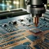
a. Laser Drilling for Microvias
Laser drilling is essential for creating the microvias used in HDI PCBs, but it requires extreme precision to ensure accurate placement and depth control. Even a slight deviation in the laser's focus can result in faulty connections or damage to the layers of the PCB. Manufacturers must invest in advanced laser drilling equipment and processes to achieve the necessary precision.
8
b. Lamination Process
HDI PCBs often feature multiple layers, which must be laminated together. The lamination process is critical for ensuring the integrity and durability of the board, especially when dealing with complex designs that include blind and buried vias. The use of thin substrates in HDI PCBs also increases the risk of warping during lamination, which can lead to defects or performance issues.
c. Cost Considerations
The advanced techniques and materials used in HDI PCB production, such as laser drilling and fine line etching, make these boards more expensive to manufacture than traditional PCBs. While HDI PCBs offer significant advantages in terms of performance and size, the cost factor can be a barrier for some applications, particularly in industries where budget constraints are a concern.
8
4. Benefits of HDI PCBs in Modern Applications
Despite the challenges in manufacturing, the benefits of HDI PCBs are numerous, making them an increasingly popular choice for cutting-edge applications. These benefits include:
a. Higher Component Density
One of the primary advantages of HDI PCBs is their ability to support a high component density. By using microvias, buried and blind vias, and fine traces, HDI PCBs can house more components in a smaller area, allowing for more functionality in compact designs.
b. Improved Signal Integrity
HDI PCBs offer superior signal integrity due to shorter signal paths, lower inductance, and reduced crosstalk between traces. This makes them ideal for high-speed applications, where maintaining signal integrity is crucial for performance. Industries like telecommunications and data centers, where high-speed data transfer is critical, particularly benefit from HDI technology.
c. Enhanced Reliability
HDI PCBs are designed to withstand more demanding environments, making them more reliable in applications where durability is essential. For example, in automotive and aerospace applications, where components are subject to extreme temperatures, vibrations, and other harsh conditions, the robustness of HDI PCBs ensures long-term reliability.
d. Design Flexibility
HDI PCBs offer greater design flexibility, allowing engineers to create more innovative and compact products. This flexibility is particularly valuable in industries such as consumer electronics, where the form factor and aesthetic design are just as important as functionality. The ability to design PCBs that fit into smaller and irregularly shaped enclosures opens up new possibilities for product design.
8
5. Applications of HDI Technology
a. Consumer Electronics
As mentioned earlier, HDI PCBs are widely used in consumer electronics such as smartphones, tablets, and wearable devices. These devices require small, lightweight, and powerful PCBs that can handle a wide range of functions in a compact form factor. HDI technology is what enables manufacturers to meet these requirements.
b. Telecommunications
In the telecommunications industry, HDI PCBs are used in high-frequency and high-speed data transmission equipment. The superior signal integrity provided by HDI PCBs is critical for ensuring reliable communication in devices such as 5G base stations and routers.
8

c. Automotive Electronics
HDI technology is increasingly used in automotive electronics, where the demand for advanced features like autonomous driving systems, in-car infotainment, and electric vehicle control systems is growing. These systems require compact, high-performance PCBs that can handle complex data processing and control functions.
8

d. Medical Devices
Miniaturized medical devices such as pacemakers, hearing aids, and diagnostic tools rely on HDI PCBs to function efficiently. The compact size and high reliability of HDI PCBs make them ideal for use in medical applications where space is limited, and precision is critical.
8
Conclusion
The increasing demand for smaller, more powerful, and more efficient electronic devices is driving significant advancements in PCB miniaturization and HDI technology. From consumer electronics to automotive and medical devices, HDI PCBs are enabling the creation of cutting-edge products that were once thought impossible. While there are challenges associated with the manufacturing of HDI PCBs, the benefits in terms of performance, size, and design flexibility make them a vital component of modern technology.
As industries continue to evolve, the role of HDI PCBs will only grow in importance, paving the way for even more innovative products and applications in the future. Whether it’s the next generation of smartphones, autonomous vehicles, or life-saving medical devices, HDI technology will continue to be at the forefront of technological advancement.


Recent Posts

October 26, 2016
The Most Successful Engineering Contractor


May 12, 2025
China PCB Drilling Routing machine Development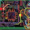
May 06, 2025
PCB Design Process and Key PointsCONTACT US
Contact US
Product Information
Quantity
Unit
Piece
Support order samples, customization, wholesale direct, and complete payment. If the product you look for does not have corresponding customized content, pls fill out the form below to contact us, and we will reply ASAP.