
Effective Strategies for ESD Protection in PCB Layout: Maximizing Performance and Minimizing Risks
Jun 02, 2023
Effective Strategies for ESD Protection in PCB Layout: Maximizing Performance and Minimizing Risks
Static electricity, a form of electrical energy that exists on the surface of objects, occurs when there is a local imbalance of positive and negative charges, such as in the case of friction-induced static discharge. Static electricity has long been a challenge for many electronic products, as the resulting discharge currents generate electromagnetic fields that can cause severe interference in circuits. Therefore, it is crucial to consider ESD protection during the initial stages of PCB design.
Principles for ESD protection in PCB layout generally involve placing ESD protection devices as close as possible to the input terminal or connector and minimizing the distance between ESD protection devices and the protected lines.
For PCB design, it is important to establish proper isolation distances at susceptible areas where static discharges are likely to occur. In the case of rack-mounted products, the breakdown distance for static voltage is approximately 1mm per kilovolt. By incorporating a 35mm isolation zone at susceptible edges, it becomes possible to withstand static voltages of up to 35kV.
1. ESD protection design for low-speed boards:
1)Route traces in a horizontal or vertical manner, minimizing the parallel arrangement of signal lines.
2)Use thicker traces whenever space allows.
3)Follow high-speed circuit design principles for routing.
4)Avoid handling critical signal lines, such as clocks and reset signals, at the PCB edges.
5)Minimize the conduction loops of all PCB traces, including power and ground loops.
6)For single-sided or double-sided boards without power planes, ensure a ground trace accompanies the power traces.
7)Whenever possible, utilize multi-layer PCB designs.
2. ESD protection design for high-speed boards:
1)Ensure a solid ground plane for routing.
2) Maintain sufficient spacing between components, such as filters, optocouplers, AC power lines, and sensitive signal lines.
3) Employ low-pass filters (C, ESD devices, RC, LC) for long-distance traces.
4) Implement isolation (adding shielding) to prevent protected wires from running parallel to unprotected ones.
5) Avoid sharing common ground paths with other components.
3. General methods to prevent static electricity:
1) Maintain the integrity of the ground plane, increase the grounding surface area, and ensure even copper distribution to maintain consistent ground resistance. Keep the ground planes at the same horizontal level.
2) Implement surrounding ground design around the PCB perimeter, enclosing data lines with a ground barrier.
3) Increase the number of grounding vias and ensure tight interconnection between ground layers.
4) Install optocouplers or transformers on the PCB, combined with dielectric isolation and shielding, to effectively suppress ESD discharge impacts.
5) Establish a single-point connection between PCB GND and the enclosure ground to prevent coupling of ESD discharge currents into the circuit via the enclosure. Carefully choose the grounding point, preferably at the cable entry point.
6) If PCB area permits and the overall system integration and ESD discharge paths are well-designed, consider implementing a protective ground ring around the PCB perimeter, with exposed copper treatment and numerous through-hole connections.


Recent Posts

October 26, 2016
The Most Successful Engineering Contractor


May 12, 2025
China PCB Drilling Routing machine Development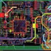
May 06, 2025
PCB Design Process and Key PointsCONTACT US
Contact US
Product Information
Quantity
Unit
Piece
Support order samples, customization, wholesale direct, and complete payment. If the product you look for does not have corresponding customized content, pls fill out the form below to contact us, and we will reply ASAP.